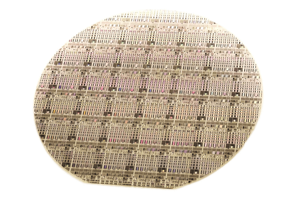
July 11 news, Xi'an University of Electronic Science and Technology, Guangzhou Research Institute of third-generation semiconductor innovation center research team in the sapphire-based enhancement of e-GaN power electronic chip mass production technology research and development breakthrough progress.
The research team overcame the entire set of mass production technologies, including ≥1200V ultra-thin GaN buffer layer epitaxy, p-GaN gate HEMTs design and fabrication, reliability reinforcement, and high-hardness material sealing and testing, and successfully developed 6-inch sapphire-based enhanced e-GaN HEMTs wafers with a threshold voltage exceeding 2V and withstanding voltage up to 3000V. The research was published in IEEE Electron Device Letters and selected as a cover highlight paper.

▲ 6-inch sapphire-based enhanced e-GaN HEMTs wafers
In this project, the research team also successfully developed an 8-inch GaN power electronic chip, proving for the first time the feasibility of mass production of 8-inch sapphire-based GaN HEMTs wafers, and breaking the traditional GaN technology is difficult to take into account the international problems of large size, high voltage resistance and low cost, which was featured in the international famous semiconductor industry magazine Semiconductor Today. Semiconductor Today”, a famous international semiconductor industry magazine.

Contact: Mandy Mao
Phone: +86 13603915493
E-mail: mandy.m@tretrust.com
Whatsapp:+86 13603915493
Add: Block C, Building 2, Star Science & Technology Park, No. 55 Zhongwei Road, Demonstration Zone, Jiaozuo City, Henan Province, China.
